Thursday, April 21, 2011

§Line Tracker : Tiny2313 based line follower robot


Hello,
          Here i am going to explain a very simple well known and Interesting project "Line Tracking Robot". Line tracker is a machine that can track a path. The path can be visible like a black line on a white surface  or it can be invisible like a magnetic field.
How to Sense Line??
Line can be Black on a White surface or White on a Black surface.To sense the line we can use LDR, IR Sensor etc. The basic concept is that when light falling on that Sensors they get activated.


When light falls on a black surface it will completely absorbed by the black surface. And when this light fall on the white surface it will be reflected through it. I am using IR Tx. Rx. pair to sense the black line. IR Tx. continuously spread IR light (Not visible to human Eye) and when this falls on IR Rx. it will generate output in millivolt.


I am using very low cost AVR series 20 pin Tiny2313 Micro-controller. We know that MCU understand TTL logic +5v for HIGH and 0v for LOW. The output of the IR sensor is fed to the MCU  pins but the output of the sensor is in millivolt ; MCU always consider it as LOW. Hence we require an Amplifier to amplify the sensor's output at TTL level.

We can use comparator which compares potentials at its Inverting and Non-inverting terminals and gives +5V or 0V signal at the output, now we can fed the output of comparator to MCU i/o pins. One major  advantage is to select Comparator as amplifier is that we can adjust the sensitivity of our sensors. LM324 is a 14-pin quad comparator IC.
LM324 Pin details
According to sensors outputs MCU takes decision and moves the Motors. Here again one thing  is to remember that the output current of MCU is not sufficient to drive the DC-Motors hence we require a Motor Driver IC. I am using very popular L293D Motor Driver IC.
Block Diagram according to above discussion-


IR Sensor and LM324 Connection.Repeat this circuit three times.The Output of LM324 is fed to the PORTD (PD0,PD1,PD2) of Tiny2313.

 Make the array of  IR sensors according to circuit below.Look the images in making steps which describes it clearly.
 
Motor Driver L293D Connections : The MCU generates outputs according to sensors input; output of MCU from PORTB(PB0,PB1,PB2,PB3) connected to pin 2,7,15,10 of L293D respectively.

  Look the table's below to understand how it work.
                

 Complete Circuit Diagram :


 Making Steps :
step:1
 step:2
 step:3
step:4
 step:5
 step:6
 step:7
 step:8
 step:9
 step:10
 step:11
 step:12
 step:13
 step:14
 step:15
 step:16
 step:17
 step:18
 step:19
 step:20

Code : Code is very basic and easy to understand for beginners. You can modify this to make more powerful.

/*Microcontroller: ATtiny2313
CPU Frequency: 1MHz Internal 
Compiler: WinAVR*/

#define F_CPU 1000000UL
#include <avr/io.h>
#include <util/delay.h>

#define TURN_LEFT                  0b00001011
#define TURN_RIGHT                0b00001110
#define MOVE_FORWARD       0b00001010
#define ROTATE                         0b00000110
#define MOVE_BACKWARD    0b00000101
#define STOP                               0b00001111

void delayms(uint16_t millis) {
  while ( millis ) {
    _delay_ms(1);
    millis--;
  }
}
int main(void){

  unsigned char sensor;
  
  DDRB = 0xFF;   //PORTB output port
  DDRD = 0x00;   //PORTD input port
 
  while(1) {

    sensor = (PIND & 0x07);

    switch(sensor)
        {
            case 0x00:PORTB = MOVE_FORWARD;   //000
                             break;
   
            case 0x01:PORTB = TURN_RIGHT;            //001
                            break;
   
            case 0x02:PORTB = MOVE_FORWARD;   //010
                             break;

            case 0x03:PORTB = TURN_RIGHT;            //011
                             break;

            case 0x04:PORTB = TURN_LEFT;              //100
                             break;

            case 0x05:PORTB = MOVE_FORWARD;    //101                   
                             break;

            case 0x06:PORTB = TURN_LEFT;                //110   
                             break;

            case 0x07:PORTB = STOP;                           //111
                            break;
               
            default:PORTB = MOVE_FORWARD;   
                       break;
        }
           }
     return 0;
  }

Troubleshooting :
1.First check the IR Transmitter is working or not. IR light is not visible to human eye ; use your mobile camera to see the IR light.
2.Check the power supply using multimeter.
3.If L293D gets heated don't worry its not a problem.
4.Most important thing is to adjust the sensitivity of the sensors by varying the 10k Pots.Without proper adjustment of Pots robot doesn't move properly.
5.You can connect one extra base for LM324 to extend this Robot in Obstacle Avoiding Robot in Future the circuitry will same only IR sensors is increased and little modification.
6.If motors rotate on opposite or reverse direction then change the polarity of motors.

Downloads :

Video: LINE-TRACKER


If this article is useful for you then don't forget to leave comment.Your suggestion and questions are also invited.
                                                                                                                        ~pratyush

Sunday, February 20, 2011

§ LDR+555: Dark Sensor


Component used:

1)        9v Battery with cap

2)        ON/OFF Switch

3)        L.D.R (Light Depending Resistance)   

4)        I.C 555 with Base

5)        L.E.D (Light Emitting Diode) 5 pieces.

6)        Variable Resistance of 50K ohms

7)        P.C.B (Printed Circuit Board)

This circuit uses the inbuilt comparator of 555.LDR is a special type of resistance whose value depends on the brightness of light which is falling on it. When light falls on the LDR then its resistance decreases which results in increases the voltage at pin2 comparator compares between the input voltage from pin2 and 1/3rd of the power supply voltage. When input falls below 1/3rd then output is set high otherwise set low. When light falls on LDR its input voltage rises so we get 0 volt at pin 3, besides in poor light we get positive output at pin3 to drive LEDs.

Circuit Diagram : design the circuit using PCB-WIZARD.


PCB:
normal


real world


artwork


unpopulated

NOTE: We can also use LM358 or LM324. These are comparator ICs.
LM358 pin details


Circuit Using LM358


real world

artwork
                                                                                                                                              ~pg

Saturday, February 19, 2011

§ Difference between CPLD and FPGA


FPGAs and CPLDs are both programmable logic. The main distinction between FPGA and CPLD device architectures is that FPGAs are internally based on Look-up tables (LUTs) while CPLDs form the logic functions with sea-of-gates (e.g. sum of products). The most noticeable difference between a large CPLD and a small FPGA is the presence of onchip non-volatile memory in the CPLD. This distinction is rapidly becoming less relevant, as several of the latest FPGA products also offer models with embedded configuration memory.The characteristic of non-volatility makes the CPLD the device of choice in modern digital designs to perform 'boot loader' functions before handing over control to other devices not having this capability. A good example is where a CPLD is used to load configuration data for an FPGA from non-volatile memory.

CPLD :
1.A complex programmable logic device (CPLD) is a programmable logic device with complexity between that of PALs and FPGAs The building block of a CPLD is the macrocell.

2.CPLDs are easy-to-understand AND-OR structure, offer a single-chip solution with fast pin-topin delays, even for wide input functions.

3. Once programmed, the design can be locked and thus made secure.

4.The limited complexity (<500 flip-flops) means that most CPLDs are used for "glue logic" functions.

5.Non-volatile configuration memory. Unlike many FPGAs, an external configuration ROM isn't required, and the CPLD can function immediately on system start-up.

6.For many CPLD devices, routing constrains most logic blocks to have input and output signals
connected to external pins, reducing opportunities for internal state storage and deeply layered logic.

7.CPLDs have several programmable PLDs which are interconnected via a programmable connections at the global interconnection matrix.

8.In the CPLD way of programming several complete logic functions at once on inividual PLDs and then bringing these PLDs together via programmable connections.

FPGA:
1.Field programmable gate array.FPGA is similar to that of larger CPLDs.

2.FPGAs offer much higher complexity, up to 150,000 flip-flops, and their idle power consumption is reasonably low.

3.Since the configuration bitstream must be reloaded every time power is re-applied, design security is an issue, but the benefits and opportunities of dynamic reconfiguration, even in the end-user system, are an important advantage.

4.FPGAs offer more logic flexibility and more sophisticated system features than CPLDs: clock management, on-chip RAM, DSP functions, (multipliers), and even on-chip microprocessors and Multi-Gigabit Transceivers.

5. Use FPGAs for larger and more complex designs.

6. FPGAs typically have range of gates from tens of thousands to several million.

7.FPGAs on the other hand have individual logic blocks - each block can be programmed to implement a logic function such as AND, OR, NOT etc. These blocks are then connected via programmable switches to implement complete logic functions.

8..In the FPGA way of programming individual AND, OR, NOT logic functions and then putting them together to implement a complete logic function.

NOTE:In general CPLDs are good choice for wide combinational logic applications while FPGAs are more suitable for large state machine.(i.e. microprocessor)
                                                                                                                                                 ~pg

§ PCB design at home

Required things --
1. PCB design software - PCB Wizard
2. LASER printer
3. Mag zine paper
4. Ferric chloride
5. Copper Platted PCB
6. Hand Gloves
7. Electric iron
8. Hand drill
9. Cello Tape
10.Plastic tub
11.Small Hacksaw
12.Scale,pencil,scrubber..etc.


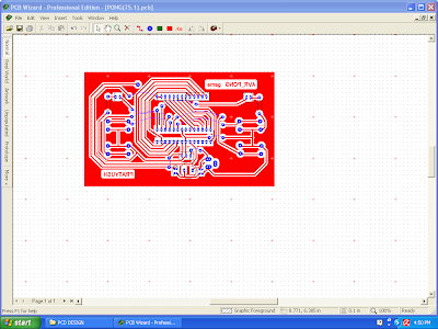
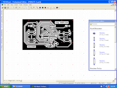
Step 1: Design your circuit in PCB Wizard software which will automatically design your PCB or you can design your PCB manually.


layout

real world

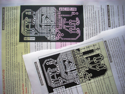
Step 2:Print the layout on magazine paper using LASER printer.
LASER printer  (CANON 2900B)
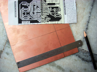
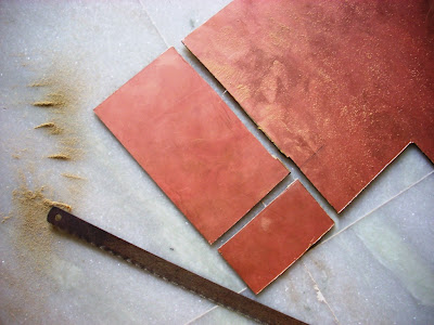
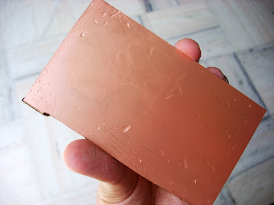
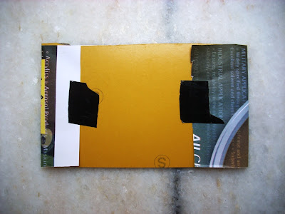
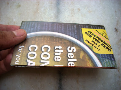
Step3. Cut the desired size of copper platted PCB using hacksaw and after cutting wash this piece. 


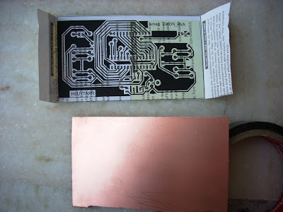
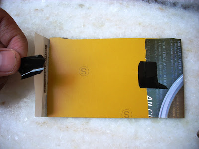
Step4.Put the paper in opposite direction on the copper platted PCB and tape it.


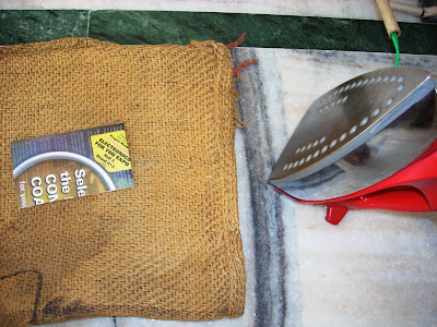
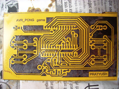
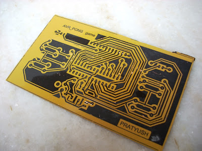
Step5.Switch on the iron set it in high HOT mode and Iron the PCB with  uniformly presser by hand about 10 min.This is very important step; if you don't do this step properly and with patience your circuit tracks get braked.(in step 7)


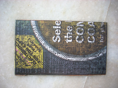
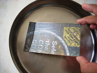
Step6. When the impression of the circuit looking outside the paper (as shown in figure below) stop doing iron and dip it into the hot water carefully and wait for 5 min.; don't touch PCB directly because it's too hot.


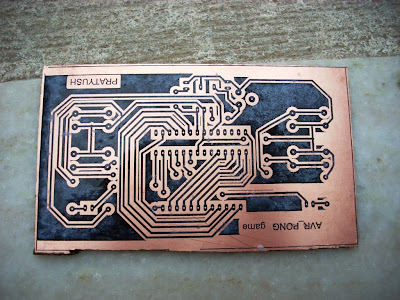
Step 7: Now keep out the PCB from water and slowly remove the paper from it. Masking of PCB is completed.


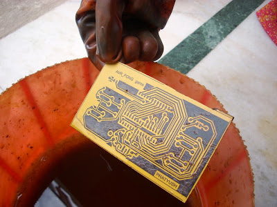
Step8: After masking it’s time for etching. For etching process etching solution is required. We can use easily available  ferric chloride. For safety use hand gloves. Take a plastic tub only not metallic otherwise the etching solution makes reaction with metal which can be dangerous for you.


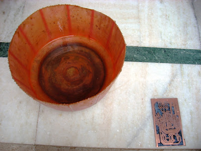
Step9: Add 4 to 6 spoon of Ferric Chloride powder in the water. The ratio of water and FeCl3 is not specific. If water is more then we have to add more FeCl3 and if water is low then low amount of FeCl3  required. One thing is remember that the water is enough for the PCB to dip completely in it. The amount of FeCl3  affect the reaction time of etching; if it is more then etching is done in less time and vice-versa. After mixing water and FeCl3 dip the PCB inside the tub and vibrate tub continuously (if u want fast etching) or after every min.


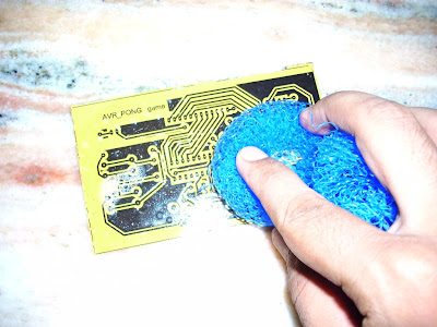
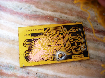
Step10: When all the copper (exposed) area vanishes then put the PCB out from the tub.Etching is done.Wash this PCB using scrubber.


Step11: Now our PCB is ready to drill. For drilling you can use small hand drill. Drill the holes.


Step12.Now the final step is to paste the components and soldered them.The final product is just looks like this.


                                                                                                                                 ~ pratyush

PID Controlled Self balancing Robot using ESP8266 and MPU6050

This ROBOT is made using ESP8266 Node MCU and MPU6050 accelerometer. Motor used here is normal gear motor of 150 rpm with TB6612FNG motor dr...