Required things --
1. PCB design software - PCB Wizard
2. LASER printer
3. Mag zine paper
4. Ferric chloride
5. Copper Platted PCB
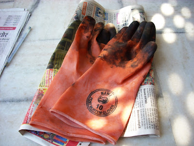
6. Hand Gloves
7. Electric iron
8. Hand drill
9. Cello Tape
10.Plastic tub
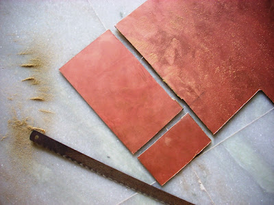
11.Small Hacksaw
12.Scale,pencil,scrubber..etc.
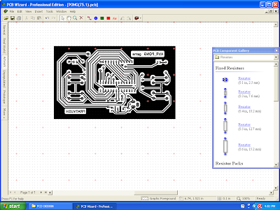
Step 1: Design your circuit in PCB Wizard software which will automatically design your PCB or you can design your PCB manually.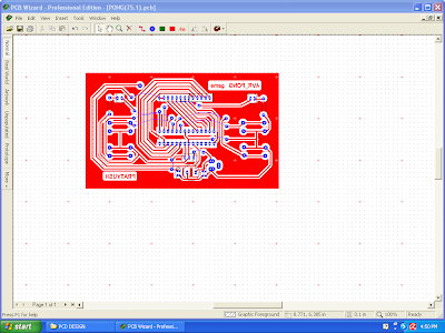
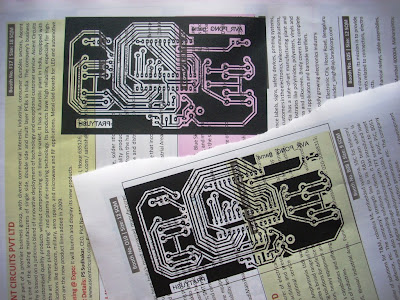
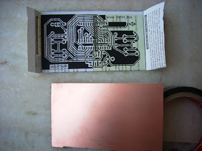
Step 2:Print the layout on magazine paper using LASER printer.
~ pratyush
1. PCB design software - PCB Wizard
2. LASER printer
3. Mag zine paper
4. Ferric chloride
5. Copper Platted PCB
6. Hand Gloves
7. Electric iron
8. Hand drill
9. Cello Tape
10.Plastic tub
11.Small Hacksaw
12.Scale,pencil,scrubber..etc.
Step 1: Design your circuit in PCB Wizard software which will automatically design your PCB or you can design your PCB manually.
 |
| layout |
 |
| real world |
Step 2:Print the layout on magazine paper using LASER printer.
 |
| LASER printer (CANON 2900B) |
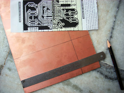
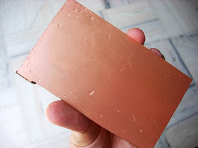
Step3. Cut the desired size of copper platted PCB using hacksaw and after cutting wash this piece.
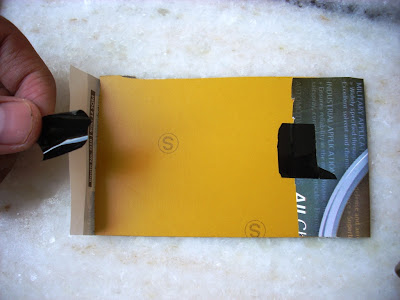
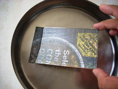
Step4.Put the paper in opposite direction on the copper platted PCB and tape it.
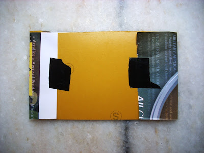
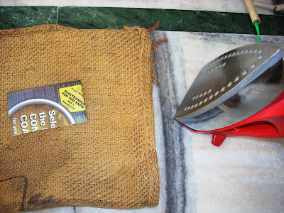
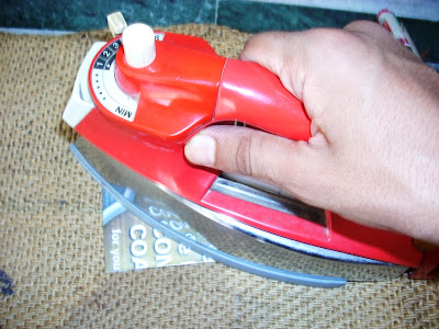
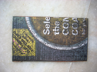
Step5.Switch on the iron set it in high HOT mode and Iron the PCB with uniformly presser by hand about 10 min.This is very important step; if you don't do this step properly and with patience your circuit tracks get braked.(in step 7)
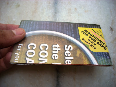
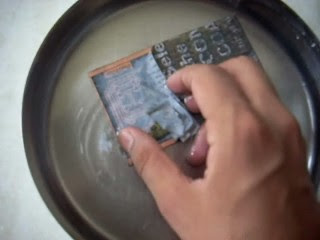
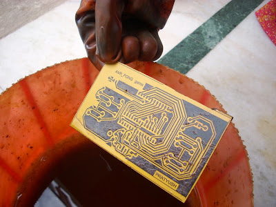
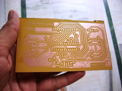
Step6. When the impression of the circuit looking outside the paper (as shown in figure below) stop doing iron and dip it into the hot water carefully and wait for 5 min.; don't touch PCB directly because it's too hot.
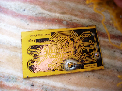
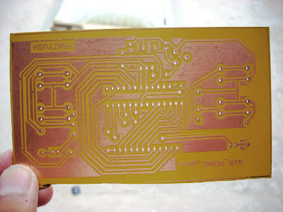
Step 7: Now keep out the PCB from water and slowly remove the paper from it. Masking of PCB is completed.
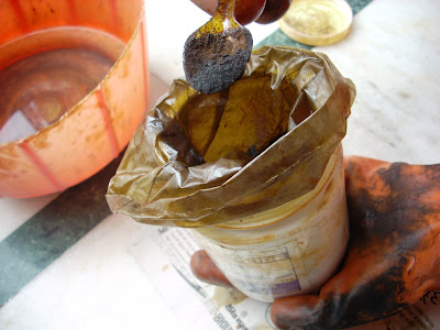
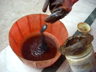
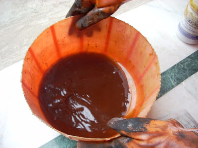
Step8: After masking it’s time for etching. For etching process etching solution is required. We can use easily available ferric chloride. For safety use hand gloves. Take a plastic tub only not metallic otherwise the etching solution makes reaction with metal which can be dangerous for you.
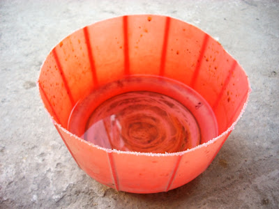
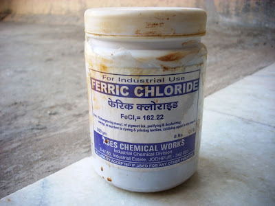

Step9: Add 4 to 6 spoon of Ferric Chloride powder in the water. The ratio of water and FeCl3 is not specific. If water is more then we have to add more FeCl3 and if water is low then low amount of FeCl3 required. One thing is remember that the water is enough for the PCB to dip completely in it. The amount of FeCl3 affect the reaction time of etching; if it is more then etching is done in less time and vice-versa. After mixing water and FeCl3 dip the PCB inside the tub and vibrate tub continuously (if u want fast etching) or after every min.
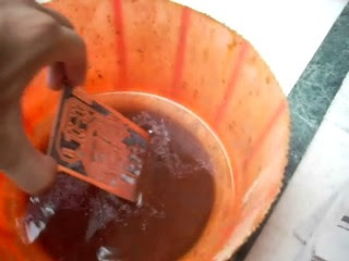
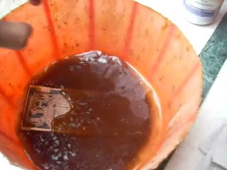
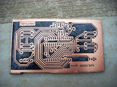
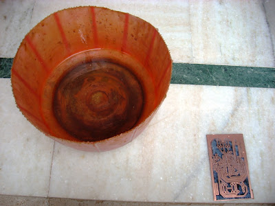
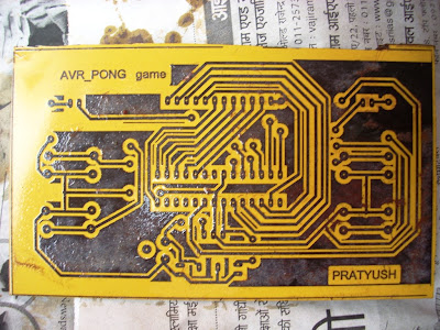
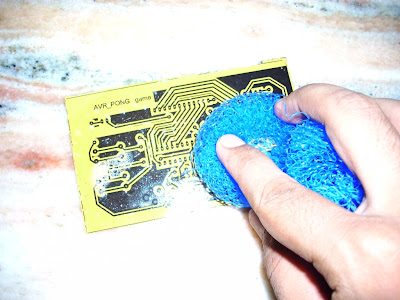
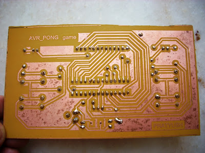
Step10: When all the copper (exposed) area vanishes then put the PCB out from the tub.Etching is done.Wash this PCB using scrubber.
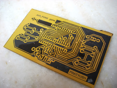
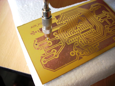
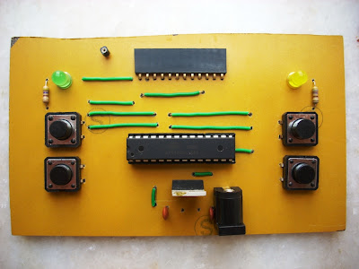
Step11: Now our PCB is ready to drill. For drilling you can use small hand drill. Drill the holes.
Step12.Now the final step is to paste the components and soldered them.The final product is just looks like this.
Step5.Switch on the iron set it in high HOT mode and Iron the PCB with uniformly presser by hand about 10 min.This is very important step; if you don't do this step properly and with patience your circuit tracks get braked.(in step 7)
Step6. When the impression of the circuit looking outside the paper (as shown in figure below) stop doing iron and dip it into the hot water carefully and wait for 5 min.; don't touch PCB directly because it's too hot.
Step 7: Now keep out the PCB from water and slowly remove the paper from it. Masking of PCB is completed.
Step8: After masking it’s time for etching. For etching process etching solution is required. We can use easily available ferric chloride. For safety use hand gloves. Take a plastic tub only not metallic otherwise the etching solution makes reaction with metal which can be dangerous for you.
Step9: Add 4 to 6 spoon of Ferric Chloride powder in the water. The ratio of water and FeCl3 is not specific. If water is more then we have to add more FeCl3 and if water is low then low amount of FeCl3 required. One thing is remember that the water is enough for the PCB to dip completely in it. The amount of FeCl3 affect the reaction time of etching; if it is more then etching is done in less time and vice-versa. After mixing water and FeCl3 dip the PCB inside the tub and vibrate tub continuously (if u want fast etching) or after every min.
Step10: When all the copper (exposed) area vanishes then put the PCB out from the tub.Etching is done.Wash this PCB using scrubber.
Step11: Now our PCB is ready to drill. For drilling you can use small hand drill. Drill the holes.
Step12.Now the final step is to paste the components and soldered them.The final product is just looks like this.
~ pratyush


???????.......
ReplyDeletenext post plz....
Hi Dude,
ReplyDeletePCBs were designed to factor in component size. Circuit needs and automated component stuffing machine capabilities to make boards that could be manufactured in large quantities to become cost-effective. I really wish u keep on giving these course with some new strategies. Keep it up..
Thanks for sharing this great article! I feel strongly about it and love learning more on this topic.pcb assembly services
ReplyDeleteHI pratyush! you and your blog was fantastic. Really impressed on your work and presentation. Every electronic engineer should follow this blog.
ReplyDeleteThank you for taking the time to make sure your content is properly written, formatted and easy to understand. I’m impressed with your writing quality.
ReplyDeletecan we use a4 size paper instead of magzine paper
ReplyDeletehello pratyush this is satyabrata dash from orissa,,,,i also make my own boards...but you see you are wasting too much of fecl3 rather dip a synthetic sponge, wide but relatively thin so that it takes less fecl3 solution to saturate,into the solution and wipe for about 2 3 5 minutes...using warm water will help you get quick etching........also use a hand drill for RS 150 only and 0.5 1 and 1mm titanium drill bits available at local tool stores ...nice and easy to work but a bit tiring.......well i have no idea how to use a wizard anyway,,,,i make mine from prints available on net or using a permanent marker available for RS20 as toner...you can correct lines and errors or breaks if any with this marker before etching.......good luck,,,,,,,,thanks anyway for the magazine paper part i previously used photo paper for RS7 each...easy way out WITH RS3,,,,wow
ReplyDelete
ReplyDeleteThanks for your great post also thanks for that your giving us great information. Please keep posting. It is a great idea. Thank you for all the information. I feel interesting to use this way.
thanks for replying pal,,,,,,you could possibly use one more way to clean toners after etching,,,,apply acetone (nail polish remover,,, no need to use lakme or other costly brands,,,,use a rs 20 nail polish remover instead it costs only half the price,,,MAKE A """PIN HOLE""" IN THE INNER SEAL)
ReplyDeleteDRIP DROP BY DROP ON COTTON AND WIPE PCB IN ONLY ONE DIRECTION AND WASH WITH WATER AND SOAP,,,,,,,SEE THE advantage
IS THAT YOU DO NOT END UP BREAKING COPPER LINES WHICH ARE TOO THIN....ALSO IT IS EASIER,,,,,,,,
BUT IT MAY SMEAR THE TONER THROUGHOUT THE BOARD MAKING IT LOOK UNTIDY,,,,,SO ITS UP TO YOU TOTALLY..
PCB designing is a great work but its hard but this blog helps me understand PCB designing
ReplyDeletehttp://goo.gl/MS4h8s
Thanks for sharing an informative post! Your given points are accurate and clearly described. Great source of information on PCB Design at home. This post will be really helpful for those who are eager to learn more about design & electrical engineers.
ReplyDeleteKeep on sharing!
Can this be used for embedded systems design
ReplyDeleteI get knowledge about how to design PCB at home with the help of your post, thx for sharing this information. prototype pcb assembly
ReplyDeleteThis comment has been removed by the author.
ReplyDeleteAwesome guide! Designing PCBs at home is super rewarding, especially when tailoring boards for custom microcontrollers. Having a reliable esp32 pinbelegung reference handy is absolutely crucial during the schematic phase to avoid routing blunders. Your step-by-step etching process makes DIY hardware development feel totally achievable for hobbyists. Great share!
ReplyDelete